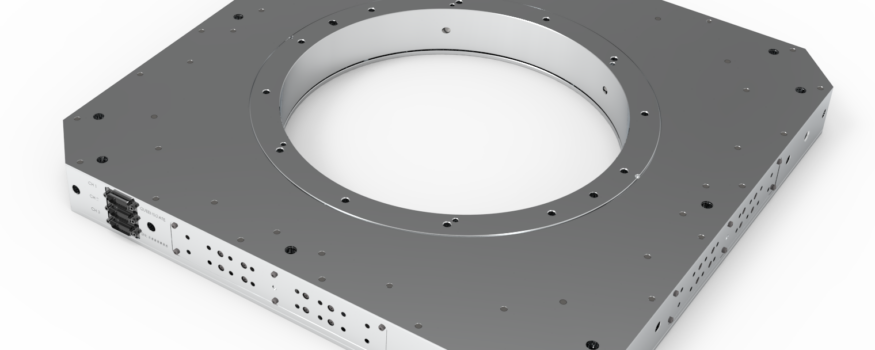
Queensgate has delivered the ‘physically largest’ piezo nanopositioning stage designed for wafer mask alignment.
The NPS-XYP-250Q 300 mm wafer–mask alignment stage provides ultra-stable and high-precision positioning of wafer masks in the 300 mm manufacturing process.
Its high-vacuum and elevated temperature capabilities make it suitable for a broad range of mask tasks both in photomask production and wafer manufacturing including vapor deposition systems.
Modern semiconductor fabrication involves aligning silicon wafers and photolithography masks to nanometre precision.
The semiconductor industry is now moving from 200 mm to 300 wafers which doubles the number of chips that can be produced from a wafer. Processing these larger and heavier wafers requires a new generation of equipment that can position wafers at nanometre precision.
This is where Queensgate’s developments in nanopositioning technology come in.
Physics World talked to Queensgate product manager Craig Goodman about producing the next generation of high-performance semiconductor devices for wafer mask alignment.


